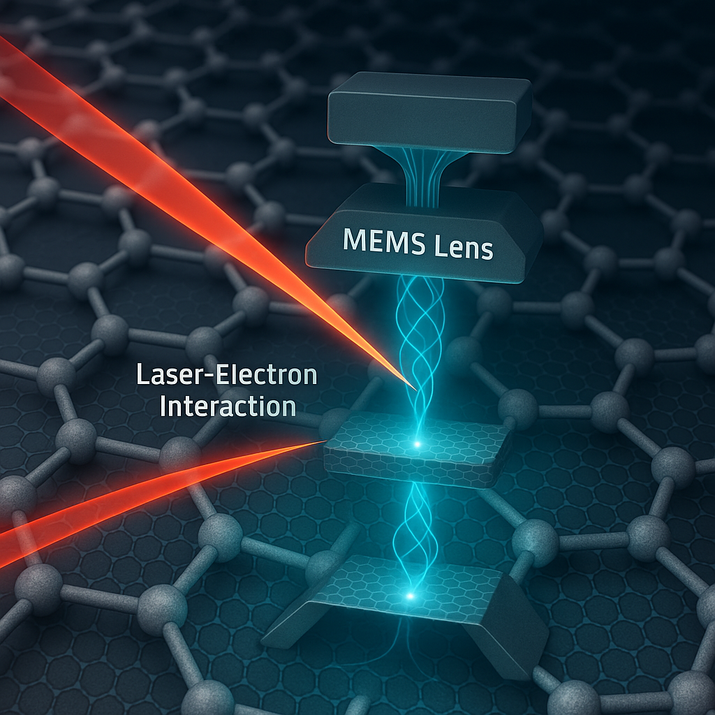
Thanks to sophisticated aberration correctors and beam monochromators that enable the accurate manipulation of the shape and energy of the electron beam, the spatial and energy resolution of electron microscopy has reached an unprecedented scale of sub-50 picometers and sub-10 meV, respectively. However, their complexity and cost, even with mEMS technology, although considerably facilitated, remain significant. This is primarily because, electrons, treated only as particles, required a complicated electron optical column to manipulate and focus them into a fine probe. Nearly all electron optics in present-day electron microscopes are described by considering the electron as a ‘tiny ball’ controlled by Maxwell’s equations.
However, there is another aspect to these “particles”, the wave nature, which is usually neglected. Such neglect overlooks a wealth of unexplored possibilities.
Applications in Science and Technology
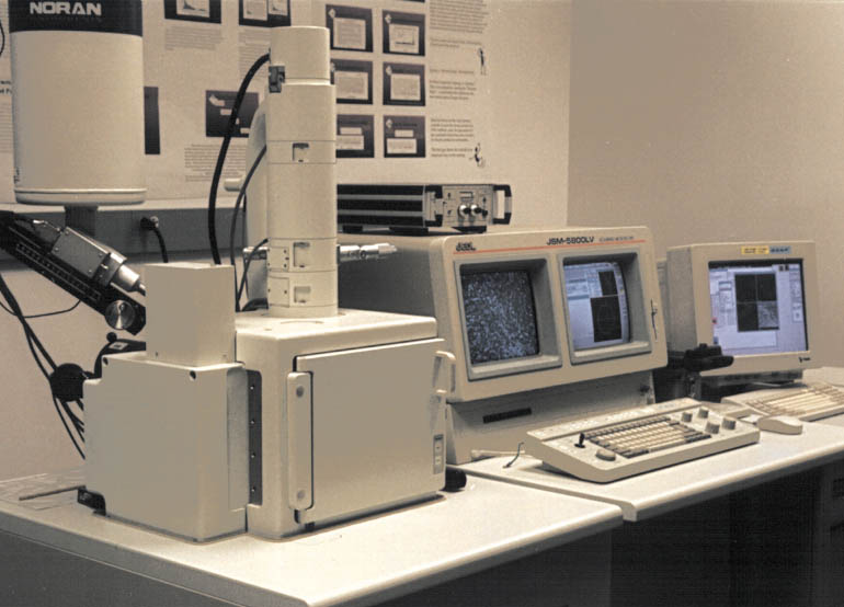
Electron Microscopy
Scanning Electron Microscopy (SEM) and (S)Transmission Electron Microscopy ((S) TEM),